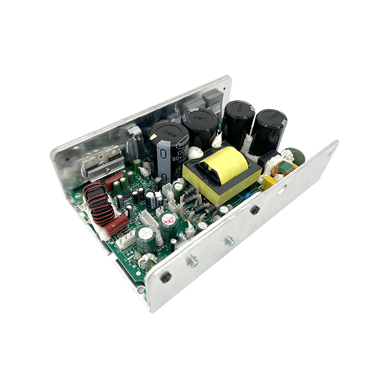
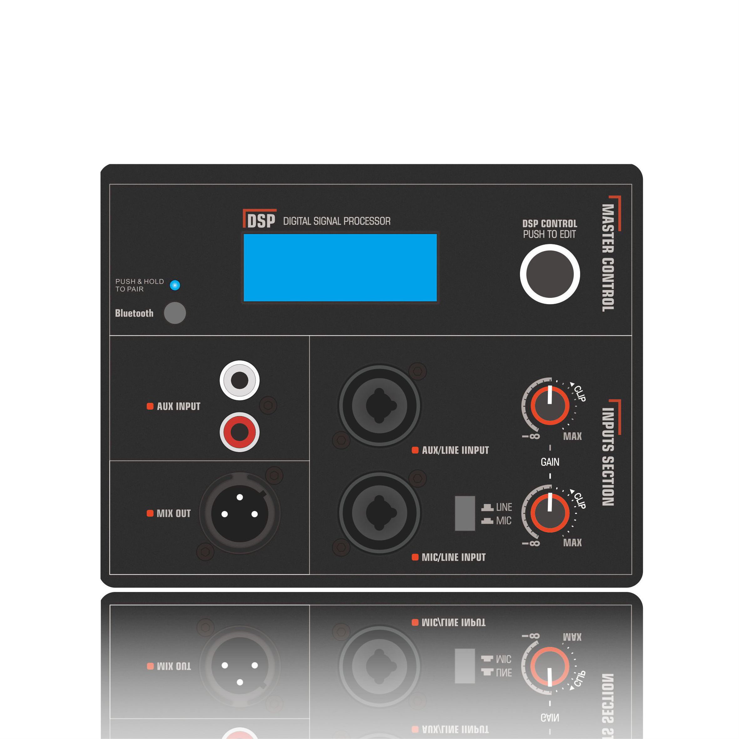
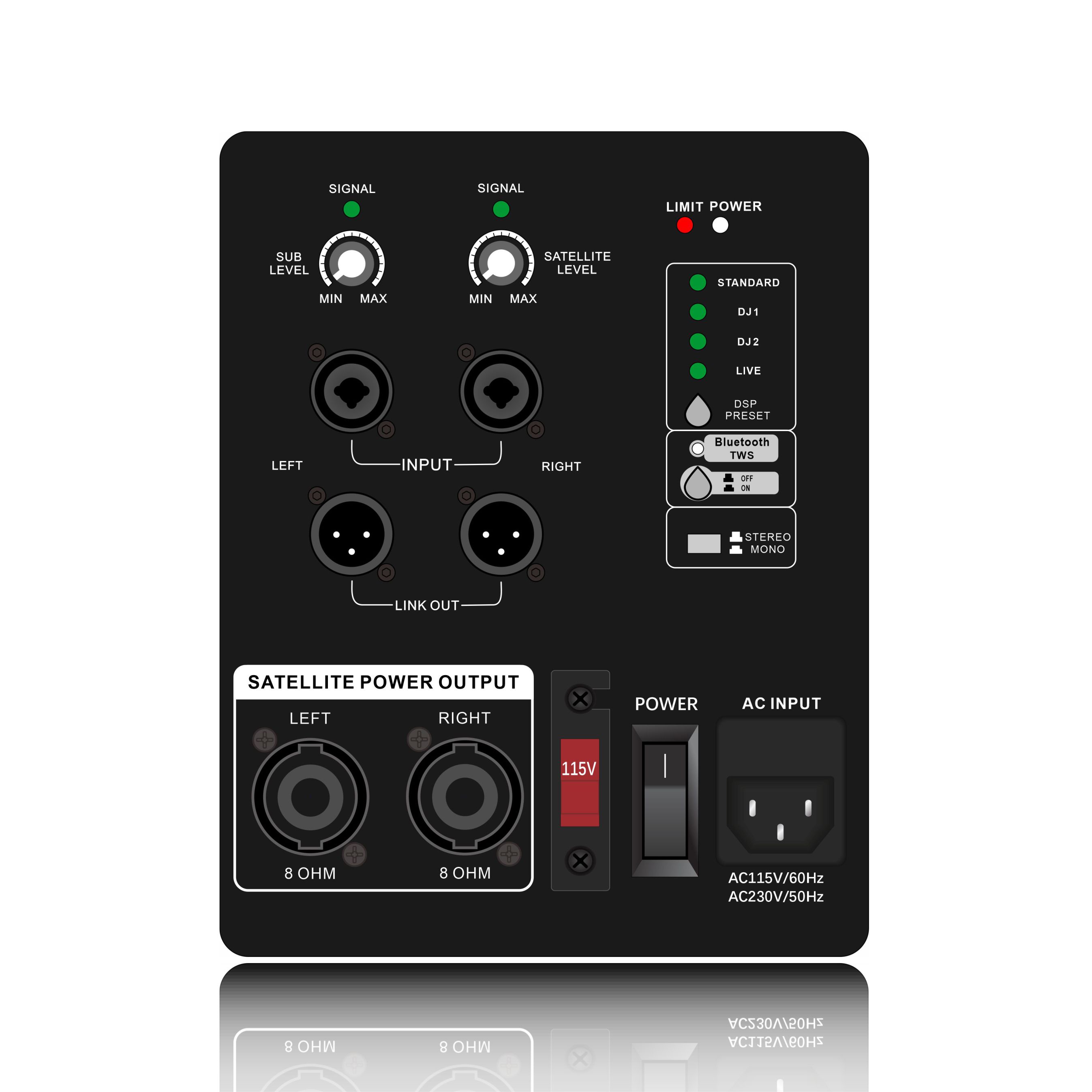
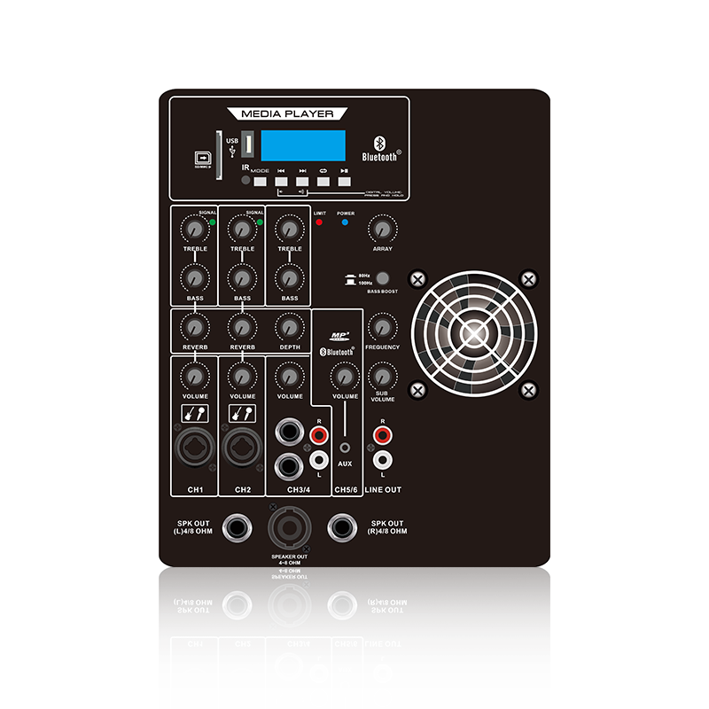
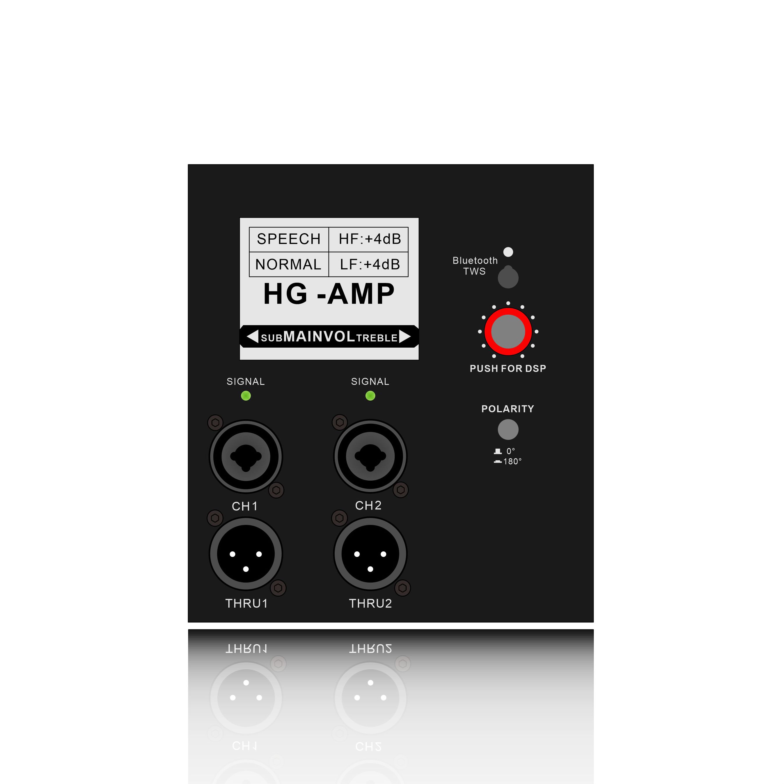
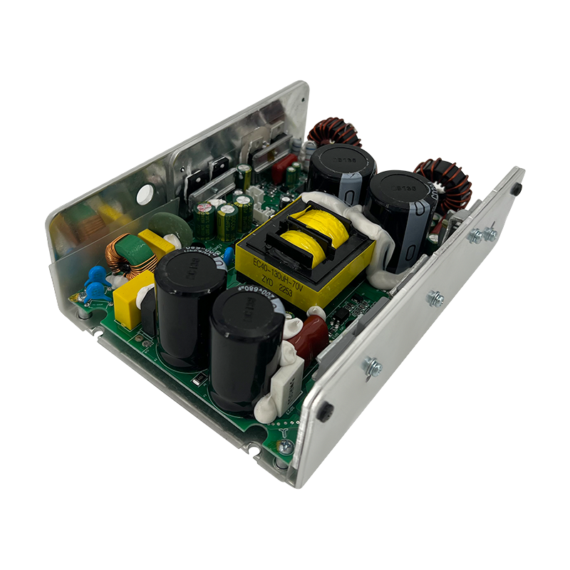
In the field of high-efficiency power conversion, the combination of LLC resonance topology and Class D amplifier is redefining the performance limit of power amplifier. Although traditional Class D amplifiers have high efficiency (usually 90%-95%), EMI (electromagnetic interference) and switching losses caused by hard switching are still insufficient. LLC resonance can push system efficiency to 98% and significantly reduce EMI by optimizing switching technology.
1. The synergistic advantages of LLC resonance + Class D amplifier
(1) The key to efficiency breakthrough: soft switching technology
The bottleneck of traditional Class D amplifier: During hard switching, MOSFET switches under high voltage and high current, resulting in significant switching losses (especially in high-frequency applications).
LLC resonance solution: Through the synergistic effect of resonant inductor (Lr), resonant capacitor (Cr) and transformer excitation inductor (Lm), the following are achieved:
Zero voltage switching (ZVS): VDS has dropped to 0 before MOSFET is turned on, eliminating turn-on loss
Zero current switching (ZCS): The current naturally returns to zero when the diode is turned off, reducing reverse recovery loss
(2) Core mechanism of EMI optimization
EMI problem of hard switching: Rapidly changing dv/dt and di/dt (such as 100V/ns) cause high-frequency radiation noise.
Smooth transition of LLC resonance: Sinusoidal resonant current (rather than square wave) reduces the switching edge slope by more than 50%, greatly reducing high-frequency harmonics.
2. Design points for achieving 98% efficiency
- Accurate matching of resonant parameters
fr needs to be slightly lower than the switching frequency (fs) to ensure that the ZVS range covers load changes. Example: In a 500W amplifier, when Lr=50μH and Cr=22nF, fr≈150kHz, and fs is set at 200kHz.
Quality factor (Q value) selection: A high Q value (>0.5) will lead to a decrease in light load efficiency. It is recommended to control it between 0.3-0.5.
- Magnetic integrated transformer design
Balance between leakage inductance and excitation inductance: Use sandwich winding or segmented winding to reduce the leakage inductance ratio to less than 5% to avoid resonance point offset.
Core material selection: Ferrite or nanocrystal is preferred for high-frequency applications to reduce eddy current loss.
- MOSFET and driver optimization
Device selection: MOSFET with low Qg (gate charge) and low Coss (output capacitance) is preferred.
Drive circuit design: Add negative voltage shutdown (-2V to -5V) to prevent false triggering caused by Miller effect.
3. Practical strategies for EMI suppression
(1) Key rules for PCB layout
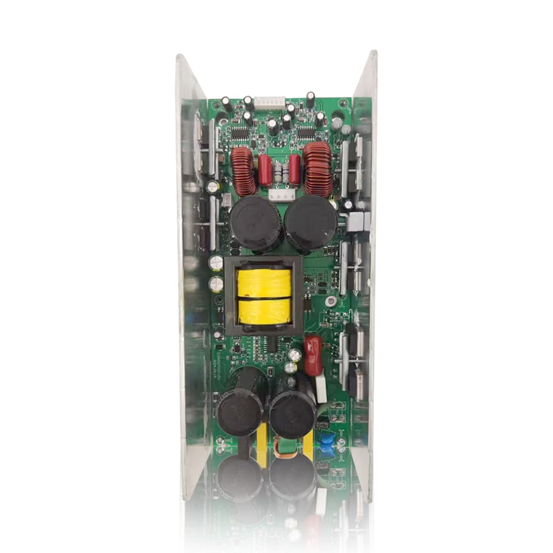
Minimize the resonant circuit: Place Lr, Cr, and transformer primary winding in adjacent areas to shorten the high-frequency current path.
Ground plane segmentation: The power ground (PGND) and the signal ground (AGND) are connected at a single point to avoid noise coupling.
(2) Filter circuit design
Input stage: Add a π-type filter (X capacitor + common mode inductor) to suppress 100kHz-1MHz conducted EMI.
Output stage: Use an LC filter (L=1μH, C=100nF) to filter out residual switching noise.
(3) Shielding and grounding
Transformer shielding layer: Copper foil wraps the transformer and is grounded to reduce magnetic field radiation.
Heat sink grounding: The MOSFET heat sink is connected to PGND through a low impedance path to avoid antenna effect.
4. Product features of LLC resonant high-reliability Class D power amplifier
- Ultra-high efficiency (>95%)
Soft switching technology: Zero voltage switching (ZVS) and zero current switching (ZCS) are achieved through LLC resonance, which greatly reduces MOSFET switching losses and the overall efficiency can reach 95%-98%.
Low conduction loss: Use low RDS(on) MOSFET or GaN devices to reduce conduction voltage drop and improve energy efficiency.
High efficiency under light load: The efficiency fluctuation is <5% in the load range of 20%-100%, which is better than the traditional hard-switching Class D amplifier.
- Excellent EMI performance
Sinusoidal resonant current: The natural sinusoidal waveform of LLC topology reduces high-frequency harmonics, and the radiated EMI is reduced by 10-15dB compared with the hard-switching Class D.
Optimized PCB layout: The key resonant loop is designed to be shortest, and with the shielding layer and filtering circuit, it can easily pass the CISPR 32/EN 55032 Class B standard.
Low noise output: THD+N (total harmonic distortion + noise) <0.05%, meeting the requirements of high-fidelity audio and medical equipment.
- Reliability design
Multiple protection mechanisms:
Overcurrent protection (OCP): real-time monitoring of output current, response time <1μs;
Overvoltage/undervoltage protection (OVP/UVP): wide input voltage range (such as 12V-60V);
Overheat protection (OTP): temperature sensor + automatic load reduction function.
Long-life components:
Solid-state capacitors (lifetime > 100,000 hours) replace electrolytic capacitors;
High temperature-resistant cores (above 130°C) avoid saturation failure.
Anti-vibration and anti-shock: potting process and metal shell design, suitable for harsh environments such as automotive and industrial.
- Compactness and high power density
Magnetic integration technology: integrating resonant inductor (Lr) and transformer (Tx) into a single core, reducing volume by 30%.
High-frequency design: The switching frequency can reach 500kHz-1MHz (GaN solution), allowing the use of smaller passive components.
Modular packaging: Standard half-brick/full-brick modules (such as 48V/500W), supporting plug-and-play.
- Intelligent and digital control
Adaptive frequency modulation: Automatically adjust the switching frequency (fs) according to load changes to maintain the optimal resonance state.
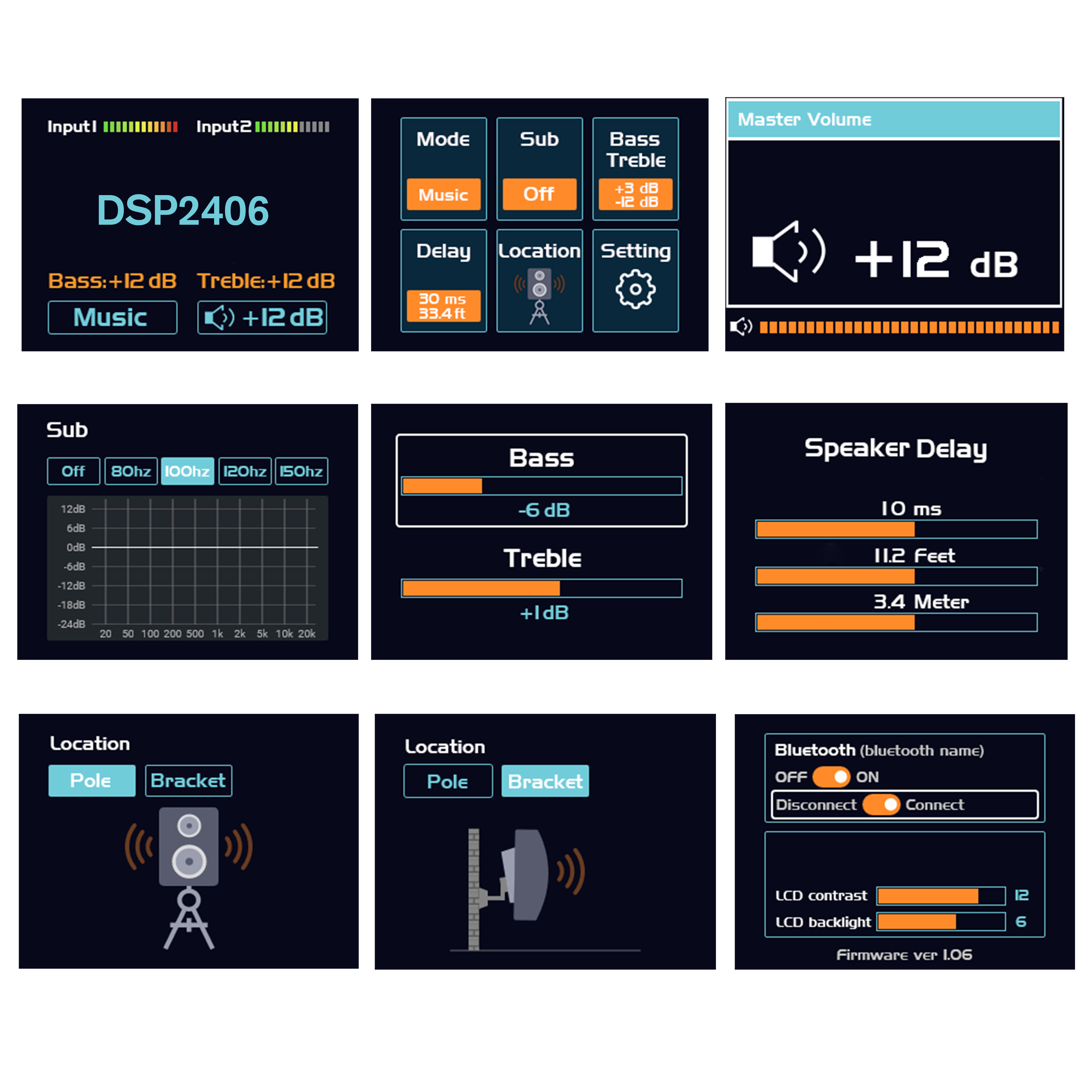
Digital interface: Support I2C/PMBus communication, real-time monitoring of efficiency, temperature, and fault status.
- Wide application adaptability
High-end audio: Hi-Fi amplifier, car audio (THD+N<0.03%);
Industrial power supply: servo drive, laser equipment (efficiency>96%);
Medical equipment: ultrasonic generator, MRI power supply (low noise & high reliability);
New energy system: photovoltaic inverter, car charger (wide voltage input).
5. Precautions for using LLC resonant high-reliability Class D power amplifiers
Although LLC resonant high-reliability Class D power amplifiers have excellent performance and stability, the following key issues still need to be noted in actual applications to ensure long-term reliable operation of the system and optimal performance:
Power supply and electrical parameter matching
- Input voltage range
Strictly follow the input voltage range specified in the specification (such as 24V-60V). Overvoltage may cause MOSFET breakdown, and undervoltage may cause resonance abnormality.
It is recommended to add a TVS diode or overvoltage protection circuit at the input end to prevent surge shock.
- Power matching
The load power must not exceed 120% (instantaneous peak) or 100% (continuous operation) of the amplifier's rated power, otherwise it may trigger overcurrent protection or damage the output stage.
For inductive loads (such as motors and transformers), an additional 20% power margin must be reserved.
Heat dissipation management
- Heat sink installation
Install a heat sink with matching specifications (such as thermal resistance ≤ 0.5℃/W), ensure that the heat dissipation surface is in close contact with the MOSFET/transformer, and apply high thermal conductivity silicone grease.
Avoid running the heat sink parallel to other high-frequency signal lines to prevent electromagnetic interference.
- Ambient temperature
The recommended working ambient temperature is ≤40℃ (industrial grade) or ≤85℃ (military grade). High temperature will significantly reduce the life of the electrolytic capacitor.
When used in a confined space, forced air cooling (wind speed ≥ 2m/s) or liquid cooling is required.
Resonance parameter calibration
- Resonance frequency (fr) verification
Before powering on, an oscilloscope + current probe must be used to verify whether the actual resonant frequency is consistent with the design value (such as 150kHz±5%). Excessive deviation will cause ZVS failure.
If the frequency is offset, it can be corrected by adjusting the resonant capacitor (Cr) or inductor (Lr).
- Light load protection
LLC resonance may leave the ZVS area when the load is <10%. The burst mode or frequency jump function needs to be enabled to avoid a sudden drop in efficiency.
PCB layout and wiring
- Key loop design
The resonant loop (Lr-Cr-transformer) must be short and wide, with a recommended length of <3cm to reduce the influence of parasitic inductance.
The power ground (PGND) and signal ground (AGND) use star-shaped single-point grounding to avoid ground bounce noise.
- EMI suppression
The input/output cables need to be equipped with magnetic rings and use twisted pair or shielded cables.
Sensitive signal lines (such as feedback lines) should be kept away from high-frequency switching nodes (spacing ≥5mm).
Protection function test
- Protection threshold verification
When using for the first time, it is necessary to simulate and test whether the overcurrent (OCP), overvoltage (OVP), and overtemperature (OTP) protections are triggered normally (such as gradually increasing the voltage with an adjustable load/power supply).
The protection response time should be <10μs (overcurrent) and <1ms (overheating).
- Fault recovery
After the fault is cleared, it is recommended to delay 1-2 seconds before re-powering on to avoid repeated shocks that may damage the device.
Maintenance and life management
- Regular inspection
Every 6 months, check whether the electrolytic capacitor is bulging and whether the magnetic component is discolored (a sign of high-temperature aging).
Use a thermal imager to scan key components (such as MOSFET, transformer) for abnormal temperature rise.
- Life prediction
Record the operating time and temperature data. When the capacitor equivalent series resistance (ESR) increases by ≥50%, it needs to be replaced.
Application taboos
No-load operation is prohibited: it may cause the resonant voltage to run out of control and damage the MOSFET.
No output short circuit: even with OCP protection, frequent short circuits will still shorten the device life.
Avoid humid/dusty environments: it may cause discharge or insulation failure (IP65 or above protection is required).
6. LLC resonant high reliability class D power amplifier FAQ
Basic principles
Q1: What is the essential difference between LLC resonant class D power amplifier and traditional class D power amplifier?
A1: Traditional class D uses hard switching, which has significant switching loss and EMI problems; LLC resonance achieves high efficiency (>95%) and low EMI through soft switching technology (ZVS/ZCS), while using sinusoidal resonant current to reduce noise.
Q2: Why can LLC resonance improve reliability?
A2:
Soft switching reduces MOSFET stress and extends device life;
Resonant topology naturally suppresses voltage/current spikes;
Multiple protection circuits (OCP/OVP/OTP) achieve rapid fault isolation.
Design application
Q3: How to select resonant parameters (Lr, Cr, Lm)?
A3:
The resonant frequency fr=1/(2π√(LrCr)) is usually set to 0.7-0.9 times the switching frequency fs;
The excitation inductance Lm is recommended to be 3-5 times Lr (to ensure that the ZVS range covers load changes);
Reference design tools (such as TI's LLC Calculator) assist in calculation.
Q4: What are the taboos in PCB layout?
A4:
Avoid too long resonant loop routing (>3cm);
Do not mix power ground and signal ground;
Keep high-frequency switching nodes away from feedback lines.
Performance optimization
Q5: What should I do if the efficiency drops at light load?
A5:
Enable Burst Mode or frequency modulation;
Optimize dead time (usually 50-100ns);
Select low Qg GaN devices to reduce drive losses.
Q6: How to further reduce EMI?
A6:
Add common-mode choke and X/Y capacitors;
Use shielded transformer and metal casing;
Avoid sensitive frequency bands (such as AM broadcast band) for switching frequency.
Troubleshooting
Q7: No output after power-on, what is the possible reason?
A7:
Check whether the input voltage is within the allowable range;
Confirm whether the enable signal (EN) is activated;
Detect whether the protection circuit is falsely triggered (such as overvoltage latch).
Q8: How to prevent MOSFET from overheating and burning?
A8:
Ensure good contact of the heat sink (thermal grease thickness <0.1mm);
Verify whether ZVS is achieved (observe VDS waveform with an oscilloscope);
Check whether the gate drive voltage is sufficient (usually 10-12V).
Application scenarios
Q9: Can it be used for battery-powered devices?
A9: Yes, but please note:
Choose a wide input voltage model (such as 8-40V);
Enable energy-saving mode when light load;
Preferentially use low quiescent current control IC (such as <1mA).
Q10: How to ensure safety in medical equipment?
A10:
Through medical-grade isolation transformers (such as 5kV withstand voltage);
Redundant design of key protection circuits;
Comply with IEC 60601-1 safety standards.
Maintenance and life
Q11: How often do electrolytic capacitors need to be replaced?
A11:
About 5-8 years under normal conditions (40°C);
Replacement is required every 2-3 years under high temperature conditions (>85°C);
Monitor the ESR value and replace it immediately if it increases by 50%.
Q12: How to determine the aging of magnetic components?
A12:
Observe whether the core is cracked or discolored;
Test whether the inductance decreases by more than 10%;
Use a thermal imager to detect local overheating (>120°C requires replacement).

 English
 Español
 中文简体
中文简体
